
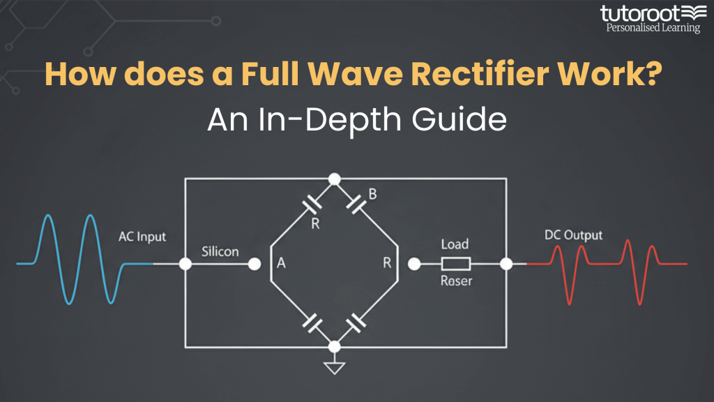
How does a Full Wave Rectifier Work? An In-Depth Guide
Introduction
Electric circuits convert alternating current into direct current, and engineers call these circuits rectifiers. There are two types of rectifiers, they are half-wave rectifiers and rectifier circuits. A half-wave rectifier loses a significant amount of power and is thus unsuitable for applications that require a smooth and continuous supply. We employ full-wave rectifiers for a smoother and more consistent supply.
Let us know more about this rectifier circuit, in this article, along with its circuit diagram
What is a Full-Wave Rectifier Circuit?
While we have understood the basic function of a rectifier, we also know that the rectifiers come in two kinds – half-wave and full-wave rectifiers.
A full-wave rectifier circuit transforms both halves of each alternating wave cycle (Alternating Current) into a pulsing DC (Direct Current) signal.
Therefore, Engineers use rectifier circuits to convert alternating current (AC) into direct current (DC) efficiently.
Please check the rectifier circuit diagram for a clearer understanding through the illustration
Types of Rectifier Circuits
Moreover, full-wave rectifiers come in two types:
- Centre-tapped full-wave rectifier
- Full-wave bridge rectifier
Understanding the difference between these two types helps students clearly understand how a rectifier circuit works.
In a center-tapped rectifier circuit, the system is made up of a center-tapped transformer, two diodes, and a resistive load. Whereas, under Full Wave Bridge Rectifier, the architecture features four diodes or more, and the resistive load. The diodes are named A, B, C, and D, and form a bridge circuit.
Circuit Diagram
There are two ways in which a rectifier circuit circuit can be built. The first technique involves a transformer with a central tap and two diodes. This design is known as a center-tapped full-wave rectifier. Check the Rectifier Circuit Diagram for a better understanding.
The second approach employs a conventional transformer with four diodes placed in a bridge configuration. This is referred to as a bridge rectifier. In the next part, we will solely cover the center-tapped rectifier circuit circuit. You may learn about bridge rectifiers in depth by reading our page on bridge rectifiers.
Circuit Diagram of a Rectifier
schematic rectifier circuit circuit diagram appears below.
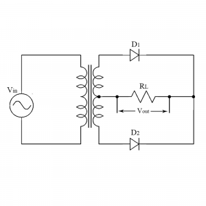
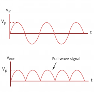
The Diagram of a Full-Wave Rectifier Circuit is shown above. The working of a full wave rectifier and Output Waveform of the Rectifier is discussed further,
output waveform
The diagram below shows the output waveform of a rectifier circuit.
A keen observation of the full-wave rectifier circuit diagram makes it clear that the circuit of the full-wave rectifier comprises a step-down transformer and two diodes. These are connected and centre-tapped. The circuit produces output voltage across the connected load resistor.
Working of the Rectifier Circuit
The rectifier circuit’s input AC is exceptionally high. The rectifier circuit’s step-down transformer transforms high-voltage alternating current to low-voltage. The anode of the center-tapped diodes is connected to the secondary winding of the transformer and the load resistor. The top half of the secondary winding becomes positive during the positive half cycle of the alternating current, while the second half of the secondary winding turns negative.
During this process, Diode D1 is forward-biased during the positive half cycle because it is linked to the top of the secondary winding. In contrast, diode D2 is reverse-biased since it is connected to the bottom of the secondary winding. As a result, diode D1 will conduct as a short circuit, and D2 will not as an open circuit.
Since the top half of the secondary circuit becomes negative, and the bottom half becomes positive during the negative half cycle, diode D1 is reverse biased and diode D2 is forward biased. Hence, the circuit produces DC voltage during both positive and negative half cycles.
Rectifier Formulae
These are some characteristics of the rectifier circuit
Peak Inverse Voltage
Peak inverse voltage is the greatest voltage that a diode can endure when reverse-biased before breaking down. The full-wave rectifier’s peak inverse voltage is twice that of a half-wave rectifier.
Where, \(D_{1} + D_{2}=2 V_{max}\)
DC Output Voltage
\(V_{dc} = V_{dc} R_{L} = V_{avg} R_{L}\)
RMS Value of Current
The current RMS value may be determined using the following formula:
\(I_{RMS} = \frac{ I_{max} }{ \sqrt{2} }\)
Form Factor
The full-wave rectifier circuit form factor is computed using the following formula:
\(K_{f} = \frac{RMS value of current}{Average value of Current}= \frac{ I_{rms} }{ I_{dc} }= \frac{ \frac{ I_{max} }{ \sqrt{2} } }{ \frac{2 I_{max} }{ \pi } }= \frac{ \pi }{2 \sqrt{2} } =1.11\)
Peak Factor
The peak factor of a full-wave rectifier circuit is given by the following formula:
\(K_{p} = \frac{Peak value of current}{RMS value of Current}= \frac{ I_{max} }{ \frac{ I_{max} }{ \sqrt{2} } }= \sqrt{2}\)
Rectification Efficiency
The following formula may be used to calculate the rectification efficiency of a full-wave rectifier:
\(\eta = \frac{DC output power}{AC Output Power}\)
Where the efficiency of the full wave rectifier is 81.2%.
These efficiency and ripple factor concepts are part of standard electronics curricula.
Ripple Factor Explained
What is a ripple?
It is an undesirable or unwanted remainder AC component coming from the conversion of the AC voltage waveform to that of the DC.
Although engineers try to remove AC components, small amounts remain at the output. These cause the DC waveform to pulsate. We refer to this unwanted component as ‘ripple’. To quantify the effective way in which the half-wave rectifier converts the AC voltage into DC voltage, we use the ripple factor – γ or r.
Therefore, The ripple factor denotes the ratio between the RMS value of the AC voltage (on the input side) and the DC voltage (on the output side) of the rectifier.
Ripple Factor Formula
\(\gamma = \sqrt{ ( \frac{ V_{rms} }{ V_{dc} } )^{2} -1}\)
- Vrms denotes the RMS value of the AC component
- Vdc refers to the DC component in the rectifier
In a center-tapped full-wave rectifier, Therefore, the ripple factor equals 0.48.
(i.e. γ = 0.48).
Why reduce the full wave rectifier ripple factor?
This is crucial to reduce the full wave rectifier ripple factor, As a result, to engineer and construct an efficient rectifier. In this case, the ripple factor should be as low as possible. Here comes the essentiality of capacitors or inductors that significantly reduce the ripples in the circuit.
Advantages and Disadvantages of the Rectifier
Advantages of This Rectifier Circuit
- The ripple frequency of this rectifier circuit is double the input frequency.
- The high output DC power.
- The ripple factor of the rectifier output is lower.
- Increased output voltage.
- A higher factor of utilization for transformers.
- Easier to offer smooth ripple frequency.
Limitations of Rectifier Circuits
- More intricate than a half-wave rectifier.
- More diodes are required: two for the center tap rectifier and four for the bridge rectifier.
- The diode has a higher PIV rating.
- Higher PIV diodes are greater in size and significantly more expensive.
- The center tap transformer is expensive.
- The center tap on the secondary winding of this rectifier is difficult to detect.
- When just a modest voltage needs to be rectified, the full-wave rectifier circuit is ineffective.
Final Notes
This article comprehensively covers information about AC to DC conversion circuits that includes explanations and formulae concerning rectifier waveforms and ripple factor behaviour. Also, we hope the Diagram of a Full-Wave Rectifier Circuit and the full wave rectifier circuit diagram were of immense use to you.

Tutoroot’s Physics online tuition classes will help you learn more about full-wave rectifiers. We have skilled teachers, who are IIT alumni to assist you in your learning journey. Transform the way you learn with Tutoroot by availing the benefits of effective personalised 1-to-1 tutoring.
FAQs
Q1. What is the efficiency of this rectifier circuit?
A full-wave rectifier has a rectification efficiency of 81.2%, which is higher than that of a half-wave rectifier.
Q2. What is the ripple factor of the rectifier output?
The ripple factor of a full-wave rectifier is 0.482, indicating lower AC ripples in the DC output.
Q3. What is the peak inverse voltage (PIV) of the rectifier?
The peak inverse voltage of a full-wave rectifier is 2Vm, where Vm is the maximum secondary voltage of the transformer.
Q4. Where is this rectifier circuit used?
Full-wave rectifiers are widely used in:
-
Mobile phone chargers
-
Laptop power supplies
-
Adapter and power supply circuits
-
Electronic devices requiring smooth DC output
Q5. What does ripple factor mean in rectification?
Ripple factor refers to the unwanted AC component present in the DC output after rectification. It measures how effectively a rectifier converts AC voltage into DC voltage.
It is defined as the ratio of the RMS value of the AC component to the DC component of the output voltage.
Q6. What is the formula for ripple factor of a rectifier?
The ripple factor of a full-wave rectifier is calculated using the formula:
Where:
-
Vrms = RMS value of the AC component
-
Vdc = DC output voltage of the rectifier