
Complete Guide to PN Junction Diode 2024 – Definition, Characteristics
A PN junction diode, as the name itself suggests, is an interface that acts as a boundary between two types, P and N, especially inside a semiconductor. This diode is created by a method called doping. This process is possible because the P diode has an excess number of holes, and the N diode has an excess number of electrons. Moreover, the region formed between the two diodes is also known as the depletion region, where both positive and negative charges are located on either side of the junctions.
In this article, let us delve deeper into the PN Junction Diode and understand forward bias and backward bias, besides learning about PN Junction Diode Characteristics specifically.
PN Junction Diode
A semiconductor is a material with its conductivity lying between conductors and insulators. Semiconductors fall under the category of intrinsic and extrinsic semiconductors, where the latter are sub-segmented as N-type and P-type semiconductors. Where a junction is created between these two semiconductors, it is referred to as P-N Junction. A diode in this regard is a device that regulates the electric flow inside a circuit.
P-N Junction Diode Diagram
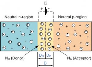
From the above P-N junction diode diagram, as you can see, the blue region represents the neutral n-region or the N diode in the semiconductor. While the orange color represents the neutral p-region or the n diode. And you can also observe that the n-diode is filled with positive electrons, and the p-diode is full of negative electrons. And the region in between where the positive and negative regions come in contact is the depleted region.
Formation of P-N Junction
The P-N junction is created through the doping method where the p-side has an excess of holes, and the n-side features an excess of electrons.
When we employ multiple semiconductor materials to create a P-N junction, a grain boundary is created that restricts electrons’ movement in two ways. This happens due to the scattering of electrons and holes, which is called doping. What follows the formation of the PN junction are – diffusion and drift. These confirm the difference in the concentration of holes and electrons on both sides of the junction. The holes from the p-side diffuse towards the n-side, whereas electrons on the n-side diffuse to the p-side. This results in the diffusion current across the junction.
PN Junction Diode Working
Firstly, to understand how a PN junction diode works, we need to learn more about the two operating systems, and the general bias conditions.
Zero Bias
There is no external voltage applied in this semiconductor, which means there is no change in the state of electrons or diodes.
Forward Bias
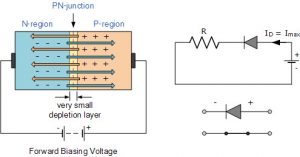
In simple, The P-N junction is categorized under forward bias when the p-type is connected to the positive terminal of the battery and the n-type is hooked to the negative one. There is the built-in electric field at the p-n junction and the applied electric field, which will be in opposite directions in case of forward bias.
Typically, in the forward bias of a semiconductor circuit, the p-type diode is connected directly to the positive terminal, and the n-type diode is connected to the negative terminal. This type of semi-conductor circuit is known as forwarding bias. Moreover, once the electricity is turned on, the different electric fields are acting in opposite directions. However, in the case of forward bias, the resultant magnitude of the electric field is lesser, which means the depleted field observed in the circuit will be thinner.
So as the applied voltage is increased, the depleted region in the semi-conductor will attain a negligible state. At a point when the resistance of the depletion area becomes negligible, it facilitates the free flow of current.
In forward bias, the key components that you learn about are battery-induced electric field, built-in electric field, conventional current, and electron current
Reverse Bias
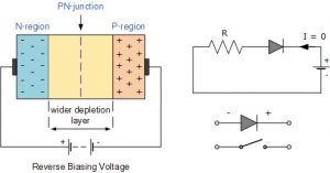
In the reverse bias of the P-N Junction, the p-type is connected to the battery’s negative terminal, and the n-type is connected to its positive side. Here, the built-in electric field and the applied electric field are spotted in the same direction. As the two fields integrate, it results in the formation of an electric field that lies in the same direction as the built-in electric field. This creates a more resistive and far thicker region of depletion. This region becomes more resistive and thicker when the applied voltage gets larger.
So, as you can guess from the above sections, in the reverse bias of the PN Junction, the p-type diode is directly connected to the negative terminal, whereas the n-type diode is linked to the positive terminal. Unlike the forwards bias system, in the case of reverse bias, both the built-in electric field, as well as the electric current is in the same direction, which in turn creates more resistance inside the semi-conductor. That will result in the increase of the depleted region in P-N Junction. And along with the increase, the size of the depleted region will also increase.
In case of reverse bias, please make note of the following aspects for improved learning – battery-induced electric field and built-in electric field
PN Junction Diode Characteristics
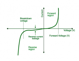
The above picture will help you understand the characteristics of the PN junction diode, and how they vary along with the change in the current(I) and Voltage(V). Besides, in this graph, you can also observe the three bias regions in the graph above. Of the typical P-N Junction Diode characteristics, as one can see in the graph, in the forward base region, the increase in the current and voltage will result in a non-linear curve. However, once the potential barrier crosses the diode behaves normally, as the curve becomes more linear.
And similarly, you can absorb the decrease of the depleted region, as the voltage and electricity vary. In the graph, you can see, as the reverse bias, will increase the potential barrier, with rising in electricity and current. Through this process, the Kinetic energy will rise, which in turn will end up damaging the diode, as it causes reverse current leakage and voltage breakdown, as mentioned in the graph.
To elaborate more on the P-N Junction Diode characteristics based on bias:
Zero Bias
No external voltage to the P-N junction diode at zero bias, which means the obstruction at the junction stops current from passing.
Forward bias
As explained, in The P-N junction diode when in forwarding bias, the p-type is linked to the positive terminal of the external voltage, and the n-type to the negative. The potential barrier is thinned down due to this position of the diode. At a voltage of 0.7 V for silicon diodes and 0.3 V for germanium diodes, these barriers fall to let the current pass.
In forward bias, the current grows gradually, and the curve formed will be non-linear due to the voltage supplied to the diode overpowering the barrier. After crossing the barrier, the diode functions normally, and the curve goes up faster when the external voltage rises, making way for a linear curve.
Reverse Bias
In the reverse bias of the PN junction diode, the p-type is linked to the negative terminal of the external voltage, whereas the n-type is connected to the positive terminal. Due to this, the potential barrier increases in significance. Also owing to minority carriers’ presence, a reverse saturation current occurs initially.
With the rising of the applied voltage, the kinetic energy of the minority charges rises, thus affecting the charges. At this point, the diode fails and can even result in self-destruction.
Application of PN Junction Diode
Technical applications
- In general, the PN junction diode is used as a rectifier to convert AC current into DC current
- Zener diode is a special kind of P-N junction diode is used in circuits to manage the regulation of voltage
- In electrical circuit, the diode is deployed as a switch that turns on and off small circuits inside a more complex circuit
- As a reverse-biased P-N junction diode, it is used as a photodiode since it is light-sensitive.
- LED also constitutes a distinct kind of P-N junction diode, in the case of a forward basis that emits light.
P-N junction Diode in regular uses
- It can be used as solar cells
- LED applications
- Equipment like oscillators and electric circuits
Conclusion
There are many other difficult topics like the PN Junction diode in Physics, which in general, the students will find hard to understand at first, and they must continuously practice understanding them better. If you are facing similar issues with Physics topics or other subjects, then the Online Interactive Classes offered by the Tutoroot platform might be very useful for you. As they offer expert staff guidance, the best study guides, cost-effective prices, and many more.
Frequently Asked Questions
How is a PN junction Diode formed?
As explained in the above section, the PN junction diode is formed through the doping method, which involves making sure that the P junction diode has more holes, while the n junction diode has more electrons.
What is the depletion region in the PN junction?
The Depleted region in the PN junction diode is a region where there are no mobile carriers, and it generally acts as a barrier between electrons and holes in both N and P diodes respectively.
What is a PN junction diode?
A p-n junction diode is a two-terminal semiconductor device that allows electric current to flow in just one way.
PN Junction Diode Characteristics
in the forward base region, the increase in the current and voltage will result in a non-linear curve. However, once the potential barrier crosses the diode behaves normally, as the curve becomes more linear.
And similarly, you can absorb the decrease of the depleted region, as the voltage and electricity vary. In the graph, you can see, as the reverse bias, will increase the potential barrier, with rising in electricity and current. Through this process, the Kinetic energy will rise, which in turn will end up damaging the diode, as it causes reverse current leakage and voltage breakdown, as mentioned in the graph.
What is PN Junction forward bias?
The P-N junction is categorized under forward bias when the p-type is connected to the positive terminal of the battery and the n-type is hooked to the negative one. There is the built-in electric field at the p-n junction and the applied electric field, which will be in opposite directions in case of forward bias.
What is PN Junction reverse bias?
In the reverse bias of the P-N Junction, the p-type is connected to the battery’s negative terminal, and the n-type is connected to its positive side. Here, the built-in electric field and the applied electric field are spotted in the same direction. As the two fields integrate, it results in the formation of an electric field that lies in the same direction as the built-in electric field. This creates a more resistive and far thicker region of depletion. This region becomes more resistive and thicker when the applied voltage gets larger.